An obvious weakness of the ESP8266 is the limited capability of it’s single ADC input. At best, the voltage range is 0-1 Vdc. While coupling an Arduino module to the ESP8266 solves this problem, is does introduce significant data acquisition delays for the Arduino-to-ESP8266 communication. A preferred solution uses the ESP8266 without requiring an additional processor.
The method presented here adds 4 ADC inputs, each supporting voltages from 0-5V. In addition, one true DAC output is available to replace the PWM feature used for that purpose.
And no additional processor is required.
This is a very inexpensive addition, requiring hardware that acquired for approximately 1 USD.
ESP8266 ADC Range Improvement
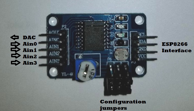
The enhancement is achieved by adding an external i2C bus ADC device to the ESP8266 system. This module, PCF8591, was added to my project recently, purchased from Ali-Express for 93 cents. It sports 4 ADC channels, one DAC channel, a potentiometer, thermister, and a photo-sensor. But for my needs, I have disabled the additional components and use it strictly as a 4-channel ADC.
The device uses an i2C bus, which requires 2 digital pins (any two) to operate.
There are two limitations I discovered while testing this module, neither of which adversely impact it’s functionality in my application.
- The ADCs and DAC are 8-bit devices. This results in a somewhat course resolution of 19mV-per-bit when using a 5V reference.
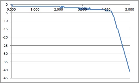
- The DAC range is linear 0-4Vdc, but compresses beyond that and tops out at 4.25Vdc.
Even with these constraints, I was still pleased to have the capability of measuring voltages 0-5V. This was a huge improvement over the ESP8266 native 0-1Vdc ADC.
The ADCs can be used single-ended (4 channels) or differential (2 channels), an added capability which allows you to measure signals with a common-mode voltage. Changing the ADC mode is a simple matter of changing the control byte when setting up the ADC for a measurement. As you will see in the sketch below, single-ended measurements are made using the control bytes:
#define PCF8591_ADC_CH0             0x40 //Measure Ain0 single-ended at CH0
#define PCF8591_ADC_CH1             0x41 //Measure Ain1 single-ended at CH1
#define PCF8591_ADC_CH2             0x42 //Measure Ain2 single-ended at CH2
#define PCF8591_ADC_CH3             0x43 //Measure Ain3 single-ended at CH3
Other options, if desired, would expand the set of control bytes:
#define PCF8591_ADC_CH0             0x40   //Measure Ain0 single-ended at CH0
#define PCF8591_ADC_CH1             0x41   //Measure Ain1 single-ended at CH1
#define PCF8591_ADC_CH2             0x42   //Measure Ain2 single-ended at CH2
#define PCF8591_ADC_CH3             0x43   //Measure Ain3 single-ended at CH3

#define PCF8591_ADC_DIFF_CH0CH3_CH0 0x50   //Measure Ain0-Ain3 differentially at CH0
#define PCF8591_ADC_DIFF_CH1CH3_CH1 0x51   //Measure Ain1-Ain3 differentially at CH1
#define PCF8591_ADC_DIFF_CH2CH3_CH2 0x52   //Measure Ain2-Ain3 differentially at CH2

#define PCF8591_ADC_MIXED_CH0       0x60   //Measure Ain0 single=ended at CH0
#define PCF8591_ADC_MIXED_CH1       0x61   //Measure Ain1 single=ended at CH1
#define PCF8591_ADC_MIXED_CH2_CH3   0x62   //Measure Ain2-Ain3 differentially at CH2

#define PCF8591_ADC_DIFF_CH0CH1_CH0 0x70   //Measure Ain0-Ain1 differentially at CH0
#define PCF8591_ADC_DIFF_CH2CH3_CH1 0x71   //Measure Ain2-Ain3 differentially at CH1
ADC Module Interfaces
The ESP8266 interface requires 4 signals:
- Vcc (5 Vdc, before the 3.3 Vdc regulator)
- Gnd (Ground)
- SDA (Any ESP8266 Digital pin – GPIO4 in this example)
- SCL (Any EAP8266 Digital pin – GPIO2 in this example)
The jumper pins (P4-P6) are removed for 4-channels ADC configuration.
Here is the minimal Arduino sketch I used to test this ADC. As you can see, the ADC read code can easily be included in a more complex sketch.
#include "Wire.h"
#define PCF8591 (0x90 >> 1)
#define PCF8591_DAC_ENABLE 0x40
#define PCF8591_ADC_CH0 0x40   //Measure Ain0 single-ended at CH0
#define PCF8591_ADC_CH1 0x41   //Measure Ain1 single-ended at CH1
#define PCF8591_ADC_CH2 0x42   //Measure Ain2 single-ended at CH2
#define PCF8591_ADC_CH3 0x43   //Measure Ain3 single-ended at CH3

#define SDA 4
#define SCL 2
byte adcvalue0, adcvalue1, adcvalue2, adcvalue3;
byte dac_value=0;
byte adc_value;

void putDAC(byte dac_value)
{
  Wire.beginTransmission(PCF8591);  //Calls the 8591 to attention.
  Wire.write(PCF8591_DAC_ENABLE);   //Send a DAC enable word.
  Wire.write(dac_value);            //Send the desired DAC value (0-255)
  Wire.endTransmission();
}

byte getADC(byte config)
{
  Wire.beginTransmission(PCF8591);
  Wire.write(config);
  Wire.endTransmission();
  Wire.requestFrom((int) PCF8591,2);
  while (Wire.available())
  {
    adc_value = Wire.read(); //This needs two reads to get the value.
    adc_value = Wire.read();
  }
  return adc_value;
}

void setup()
{
   Wire.begin(SDA,SCL);
   Serial.begin(115200);
   putDAC(0);
   Serial.println("dac,ain0,ain1,ain2,ain3");
}

void loop()
{
   adcvalue0 =  getADC(PCF8591_ADC_CH0);
   adcvalue1 =  getADC(PCF8591_ADC_CH1);
   adcvalue2 =  getADC(PCF8591_ADC_CH2);
   adcvalue3 =  getADC(PCF8591_ADC_CH3);

   Serial.print(dac_value++);
   Serial.print(",");
   Serial.print(adcvalue0);
   Serial.print(",");
   Serial.print(adcvalue1);
   Serial.print(",");
   Serial.print(adcvalue2);
   Serial.print(",");
   Serial.print(adcvalue3);
   Serial.println();

   putDAC(dac_value);

   delay(100);
}
This simple sketch configures the I2C library to attach to ESP8266 GPIO2 and GPIO4 and loop through a sequence of setting the DAC and reading all 4 ADC channels. For this setup, the DAC output is connected to all 4 ADC inputs and jumpers P4-P6 are removed. As one would expect, for each DAC setting, identical ADC values are measured for all 4 ADCs. But there are some deviations from the DAC setting:
DAC Limitations
The ADC measured values deviate from the DAC setting by no more than 1 bit (~ 20mV) from 0-2 Vdc. This deviation increases to 4 bits around 4 Vdc, with the DAC output topping out at about 4.2 Vdc.
From this we can conclude that the DAC has a functional range from 0-4 Vdc with an error no greater than 4 bits (80mV). Not super accurate, but it is adequate for many applications.
I measured the ADC output with a DVM (digital voltmeter) to confirm the DAC output never exceeded 4.2 Vdc.
ADC Voltage Range
And to confirm the ADC has a full range of 0-5VDC (0-255 byte value), I applied 5 Vdc to one of the Ain inputs and verified the measure value as 255 (5 Vdc). I also used the built-in potentiometer to swing the ADC measurements between 0 and 255 (0-5 Vdc). With a slight modification to the sketch to display the ADC readings from the potentiometer (Ain3) in Vdc, we observe good correlation between the applied voltage and the ADC measurement.
Great!
This confirms the ADC can read voltages over the full 0-5 Vdc range.
Expanding the Channels
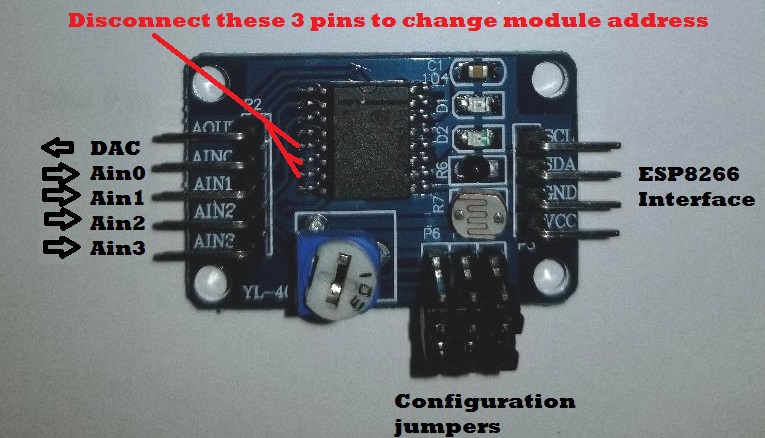
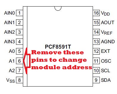
The PCF8591 ADC has 3 programmable address lines which makes it possible to expand the ADC channel count from 4 to 32. Even better, this still only requires 2 ESP8266 digital (GPIO) channels as the control pins would all be connected in parallel.
But there is a catch with the XL-40 carrier module that holds the PCF8591. The 3 address lines are hard-wired to ground. So, to expand the channels, you would need to cut the traces (lift the pins) to set a different address for each added module in your ESP8266 configuration.
No impossible, but you have to be careful not to overheat the device when desoldering the pins.
In Closing
Here is a low-cost (1 USD) addition to your ESP8266 setup that expands the ADC capability to 4 channels with the bonus of a real DAC output. While the DAC is limited to a 0-4Vdc range, you have the full 0-5 Vdc available for analog measurements with reasonable accuracy.
Hope you find this a useful addition to your projects.


